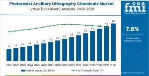
Photoresist Ancillary Lithography Chemicals Market Projected to Reach USD 4.3 Billion by 2036
The photoresist ancillary lithography chemicals market is projected to grow from USD 2.1 billion in 2026 to USD 4.3 billion by 2036, at a CAGR of 7.8%.
NEWARK, DE, UNITED STATES, January 19, 2026 /EINPresswire.com/ -- The global photoresist ancillary lithography chemicals market is poised for significant expansion, with its valuation projected to rise from USD 2.05 billion in 2026 to USD 4.3 billion by 2036. This robust growth, representing a compound annual growth rate (CAGR) of 7.8%, is fundamentally driven by the semiconductor industry’s shift toward sub-5nm process nodes and the escalating complexity of Extreme Ultraviolet (EUV) and advanced Deep Ultraviolet (DUV) lithography.
As semiconductor fabrication moves toward smaller geometries and tighter defect tolerances, ancillary chemicals—including developers, strippers, and anti-reflective coatings—have evolved from secondary consumables into yield-critical inputs. These materials are now foundational to achieving consistent pattern fidelity and line-edge roughness control in advanced logic and memory devices.
Strategic Market Dynamics: Process Integration as a Competitive Barrier
In the advanced lithography landscape, competitive power is anchored in deep process integration rather than manufacturing scale alone. Suppliers that embed their chemical sets into qualified lithography stacks defend significant pricing power, as these "processes of record" are difficult and risky for fabs to change once high-volume yield is stabilized.
• Yield Sensitivity: Even minor formulation deviations can disrupt critical dimensions, making fabs highly cautious about switching suppliers.
• Product Dominance: Photoresist Developers currently lead the market with a 32% share, driven by their essential role in defining circuit patterns after exposure across high-frequency usage steps.
• Application Focus: Logic and Foundry manufacturing accounts for 40% of demand, reflecting the high wafer volumes and multiple patterning steps required for high-performance computing and AI accelerators.
Request For Sample Report | Customize Report | Purchase Full Report -
https://www.futuremarketinsights.com/reports/sample/rep-gb-31466
Regional Growth Highlights: Strategic Supply Chains and Fab Expansion
Geographic growth is closely tracking the multi-billion-dollar fab investments in Asia Pacific, North America, and Europe, where localized supply chains for electronic-grade chemicals are becoming a national security and industrial priority.
• China (9.0% CAGR): Leading global growth through aggressive large-scale investments in domestic semiconductor fabrication and a strategic push to localize the entire electronic chemical supply chain.
• Brazil (8.6% CAGR): Emerging as a high-growth hub for specialty semiconductor processing and advanced electronics assembly, supported by increasing regional demand for precision lithography materials.
• United States (7.5% CAGR): Driven by the revitalization of domestic manufacturing and government-backed initiatives like the CHIPS Act, fueling demand for ultra-pure ancillary chemicals in advanced logic facilities.
• Germany (7.4% CAGR): A cornerstone of European semiconductor activity, focusing on high-precision manufacturing for automotive electronics and industrial automation.
• South Korea (7.0% CAGR): Sustained by the expansion of world-leading memory (DRAM & NAND) fabs that require massive volumes of ultra-high-purity developers and strippers.
Innovation and Competition: The EUV/High-NA Roadmap
The market is characterized by a limited group of elite suppliers capable of meeting the stringent purity requirements of EUV and next-generation High-NA lithography. These advanced nodes require chemicals with ultra-low trace metal content (measured in parts-per-trillion) and exceptional stability.
Industry leaders such as Tokyo Ohka Kogyo (TOK), JSR Corporation, and Shin-Etsu Chemical are at the forefront of co-developing ancillary chemistries alongside lithography tool OEMs. Other major players—including DuPont (Electronics & Imaging), Merck Group (EMD Electronics), and FUJIFILM Electronic Materials—are expanding their global footprints with fab-adjacent purification facilities to ensure just-in-time delivery and technical support. Specialized contributors like Sumitomo Chemical, ALLRESIST GmbH, Dongjin Semichem, and Micro Resist Technology continue to drive innovation in niche patterning and specialty device applications.
Hurdles to Entry: Purity and Qualification Cycles
Despite the bullish outlook, the market faces constraints due to the exhaustive qualification cycles required by semiconductor manufacturers. The validation of a new ancillary chemical can take months or even years, as any quality deviation can lead to catastrophic yield loss. Furthermore, regulatory frameworks regarding hazardous solvent handling and safer chemical alternatives are increasing the operational overhead for global distributors.
Similar Industry Reports
Photoresist Chemical Market
https://www.futuremarketinsights.com/reports/photoresist-chemicals-market
Lithography Equipment Market
https://www.futuremarketinsights.com/reports/lithography-equipment-market
Photoresist and Photoresist Ancillaries Market
https://www.futuremarketinsights.com/reports/photoresist-and-photoresist-ancillaries-market
Sudip Saha
Future Market Insights Inc.
+1 347-918-3531
email us here
Legal Disclaimer:
EIN Presswire provides this news content "as is" without warranty of any kind. We do not accept any responsibility or liability for the accuracy, content, images, videos, licenses, completeness, legality, or reliability of the information contained in this article. If you have any complaints or copyright issues related to this article, kindly contact the author above.

